Based on designs by James, W6PQL
And in particular his HF LDMOS amplifier design described here:
https://www.w6pql.com/1_kw_sspa_for_1_8-54_mhz.htm
A key part of the amplifier is the switchable low pass filter design. This is designed to suppress the odd-order harmonics in the amplifier output which would be unacceptably high without it.
Construction
I built up the filter assembly from the the pcb and components supplied by W6PQL I tested it using the well known nanoVNA and the results are set out here.
A full description of James’s design can be found here: https://www.w6pql.com/a_1.5kw_lpf_for_160-6m.htm
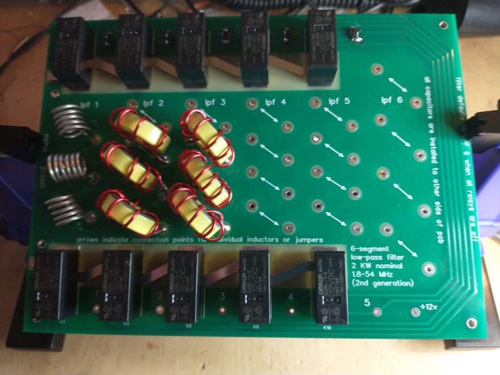
The board supports 6 different filters. With no relays energised the sixth filter for the 150m band (1.8-2MHz) is in circuit. Each of the five pairs of relays switch an alternative filter bank when energised by grounding the control inputs. The following filters are equipped:
- 160m band (default) <2MHz
- 80m band (#5) <4MHz
- 40m and 30m <10.2 MHz
- 20m and 17m bands <18.2MHz
- 15m, 12m and 10m bands < 30MHz
- 6m band <54MHz
Each of the low pass filter filter sections are 7-pole Chebyshev types which should give sufficient harmonic rejection.
The top side of the board has the relays and the toroidal coils, all except the 6m band use ferrites of different types. The bottom side has a great number of surface mount capacitors, which are easy to mount with some tweezers and patience, soldering one side at a time. (I managed to wick some solder between two adjacent capacitors to produce a hard to spot short in the 160m section which uses a lot of capacitors in parallel) But this was more or less the first time I had done much with SMD and easy to fix once spotted.
Testing
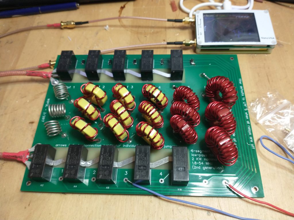
To test the assembly I made use of an inexpensive nanoVNA unit, bought from eBay. The VNA is the white box in the top right connected to a PC via a USB cable. The two SMA connectors on the VNA are cabled to the the input and output of the the filter unit. The red wire at the bottom right is feeding 12V from a bench PSU to the board. with no ground applied to the control inputs the 160m filter is in circuit. By grounding each of the five control inputs in turn with the blue wire each of the filters in turn is placed in circuit and the performance measured by the nanoVNA.
James, W6PQL has a collection of S21 gain/loss plots and S11 return loss plots on his web site. Being an ex HP engineer, I suspect he has access to a conventional high performance network analyser for his testing. However, I figured the nanoVNA would at least confirm the correct operation of the unit I assembled and highlight any errors in construction. In practice my results were very close to the example plots on the W6PQL website.
I have found it is much easier to use Ruhne Broberg’s open source software nanoVNASaver on the connected PC. Life is too short to spend too much time faffing about with the fiddly buttons and soft keys on the nanoVNA unit itself.
https://github.com/mihtjel/nanovna-saver/releases
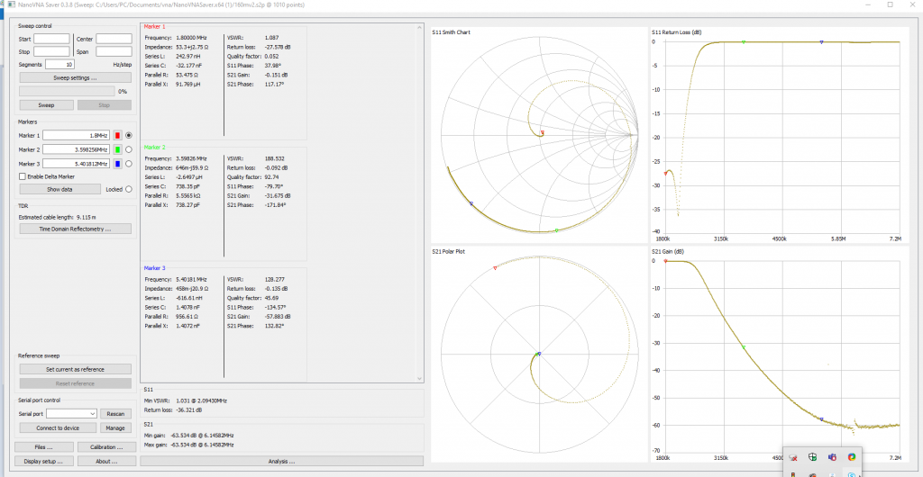
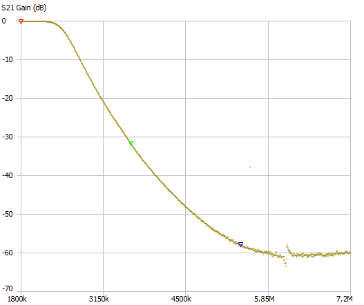
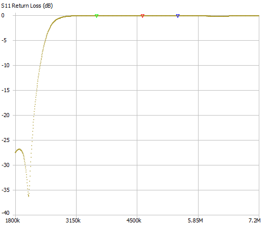
Results – 160m band
Second harmonic suppression at 3.6MHz was around -32dB and third harmonic suppression at 5.4MHz was -58dB. The in-band return loss was always better than 25dB. The filtered harmonic content will be reflected directly back to the source as the return loss at these frequencies is zero.
Results – 80m band
Second harmonic suppression at 7MHz was around -30dB and third harmonic suppression at 10.5MHz was -53dB.
Results – 40m and 30m bands
Second harmonic suppression of the 7MHz (40m band) signal at 14MHz was around -20dB and third harmonic suppression at 21MHz was -48dB.
Results – 20m and 17m bands
Second harmonic suppression of the 14MHz (20m band) signal at 28MHz was around -27dB and third harmonic suppression at 42MHz was -49dB.
Results – 15m, 12m and 10m bands
Second harmonic suppression of the 21MHz (15m band) signal at 42MHz was around -17dB and third harmonic suppression at 63MHz was -45dB.
Results – 6m band
Second harmonic suppression of the 50MHz (6m band) signal at 100MHz was around -29dB and third harmonic suppression at 150MHz was -60dB.
Performance Implications
At 1000w key down the even order harmonics in the push-pull LDMOS design are reasonable but the odd-order harmonics are truly monstrous. W6PQL reports the third order harmonic as only 10dB down on the fundamental.
The minimum suppression of third order products in these filters is around 45 dB for the compromise filter covering three bands, 15m, 17m, and 10m. So at full power we might see a third order product at aroound-55dB below the carrier (-55dBc).
This is not too bad. In the USA amateurs must achieve -43dBc in part 97 of the FCC regulations. In the UK/EU its -50dBc for commercially built equipment intended for HF Amateur Radio use (-60dBc for other services). For UK amateurs building their own equipment the licence conditions are very “British” in their avoidance of prescription saying merely “the emitted frequency of the apparatus comprised in the Radio Equipment is as stable and as free from Unwanted Emissions as the state of technical development for amateur radio apparatus reasonably permits.”
I think hitting -50dBc in looks to be more than “reasonable” to me and should be possible.
Another important point is that UK amateurs are only allowed to run at 400W (26dBW) in most bands which is 4dB less than what the amplifier to be filtered is capable of. The designer doesn’t give any harmonic output figures when the amplifier is not driven so hard. However I would expect the 3rd harmonic to fall three times as fast as the fundamental, so be reduced by a further 12dB when run at the UK limit. This would indicate a worst case 3rd harmonic output at least -67dBc under these more benign conditions.
Running at 400W should also improve the in-band intermodulation performance of the amplifier.